One of the defining traits of analog CMOS designers is the ability to implement a common-mode feedback (CMFB) loop. When the input devices on a differential pair are all NMOS (or NPN), and the loads are either inductors or resistors, a common-mode feedback loop is unnecessary, because the output resistance of the differential pair is weighted down by the low resistance of the inductor or resistors.
However, when one has a high-impedance trans-conductor (NMOS or PMOS) loaded with a high-impedance current source (PMOS or NMOS), a common-mode feedback loop becomes necessary. Even small differences between the bias current of the trans-conductor and the bias current of the load can induce large swings in voltage when multiplied by the high resistance of the output node.
This post presents a very simple and very effective common-mode feedback method.
Introduction
In a previous post, I detailed what essentially amounts to a common-mode feedback circuit. It was shown as a level-shifter, but at its core, it sense the common-mode (average between the differential outputs) and adjusted it to a reference value. If there is interest, I can detail how to apply that topology in a differential pair to create a common mode feedback loop; just post a request in the comments.
The difficulty with that approach is that it places the common-mode feedback loop directly on the output branches. Precision in the common-mode requires high gain the common-mode feedback loop. In the case where there is a capacitor load on the output branches (most of the time), this high gain causes a stability concern. The bandwidth of the gain must be lowered for stability.
There is a another way to accomplish common-mode feedback. (It has been published in a journal or conference article in the past. I will give a reference when I have access to the IEEE database.) The benefit of this approach is that it separates the precision of the common-mode voltage from stability concerns.
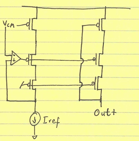
I will consider the case where we have an NMOS-input diff pair with PMOS loads. The common-mode feedback involves placing an extra set of PMOS devices that are connected together. These extra devices are biased in triode. The reference (diode-connected) branch should also have this triode device:
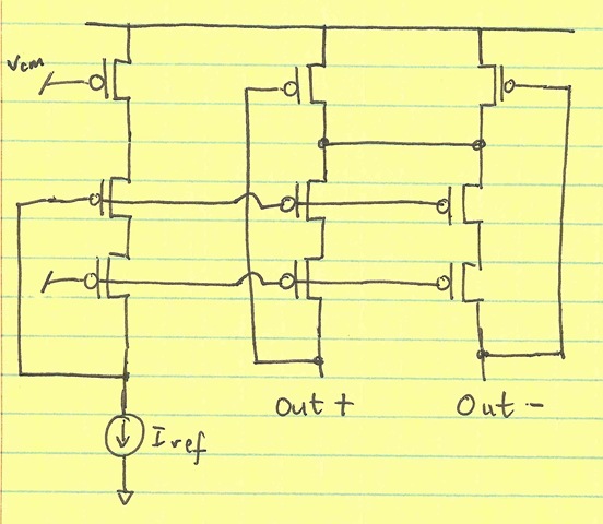
I have excluded the input NMOS diff-pair because it would clutter the sketch.
This common-mode feedback works by changing the source voltage on the PMOS current sources in proportion to the output common-mode. The connection between the two triode devices does an averaging of the two PMOS-source voltages.
Analysis
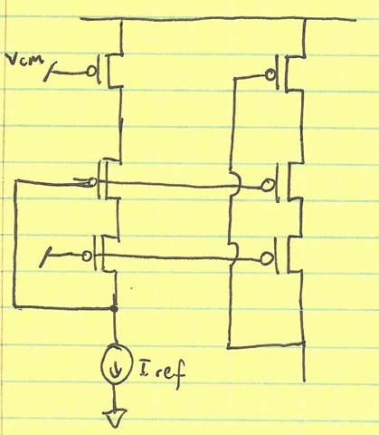
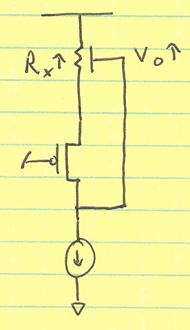
Since we are just considering the common-mode effect, we can assume a zero differential and therefore the two output branches (negative and positive) have exactly the same (in terms of both node voltages and branch currents). As a result, we don’t need to draw both branches each time. We can simply draw one branch (pick one)—or we can consider a single (equivalent) branch that is the average of the two differential branches:
Note that the reference branch has a triode PMOS device that is connected to the desired common mode, VCM. If the output branch is loaded with Iref, then the voltages will be exactly the same. Let’s now consider what happens when the output is not loaded in Iref, but something a little smaller. I’ll denote with arrows the direction that different values take. For example, if the load current has gone down:
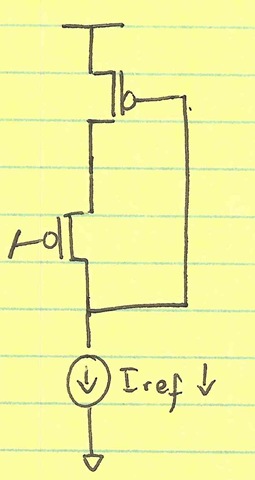
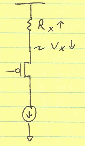
You’ll also note that I’ve done away with the cascode device as it does not affect the analysis. The load current going down will cause the output voltage to go up:
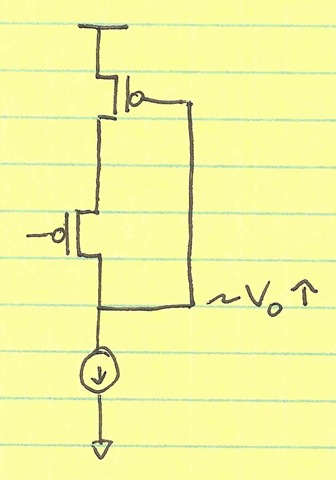
This in turn will cause the resistance of the triode PMOS to go up shown now as a voltage-controlled resistor Rx:
This increased resistance then causes the source of the PMOS to go down in voltage Vx:
The source Vx of the PMOS going down in voltage reduces the |VGS| of the PMOS device, thus reducing the voltage it puts out. Thus its output current Io is reduced:
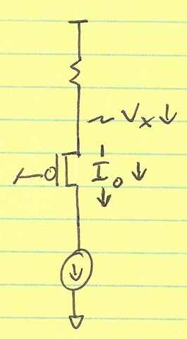
Io being reduced then causes the output voltage Vo to go down:
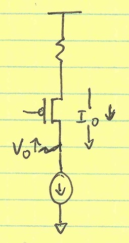
Vo going up thus negates the initial effect of Vo going up, completing a negative feedback loop. What has happened is that the PMOS side has adjusted its current to match the NMOS side, thus leaving the output voltage intact but changing the current through the branch.
One more thing
The astute reader will notice that all this negative feedback, in the end, only makes the output current Vo equal to the gate voltage on the diode connected device. It does not actually place the output voltage at the desired common-mode voltage. To do so, we need to add one more op-amp to the reference branch:
You might feel cheated at this point to learn that you still need a differential amplifier that senses and adjusts common-mode. However, the beauty of the system is that this reference branch is not operating directly on the output branch. If there are capacitors on the output branch, they are designed independently of the stability of the reference branch. As a result, one can place extremely high gain on it to get a very precise common-mode voltage without worrying about stability.
Conclusion
The output branches of an OTA already have a high gain from the gates of the current-source loads to its output. As a result, a separate high-gain stage is not necessary. The main benefit of the triode-based CMFB loop is its ability to average the common mode of two differential branches without requiring a separate summing amplifier or a resistor sense, all in a low-gain highly-stable configuration
The triode-based CMFB allows one to create a wide-band, stable common-mode feedback loop on the output branches to cancel the dynamic common mode perturbations. A separate loop handles precise bias of the current source devices to target a reference common mode. This separate loop can be made arbitrarily high gain while maintaining stability. However, this separation can also be achieved with a more typical common-mode feedback sensing amplifier configuration. (If there is interest in this topic, please post in the comments.)
The main downfall of the triode-based CMFB is that some albeit small amount of voltage is dropped across the triode devices. This drop eats up some headroom, but more importantly, it robs some voltage drop from the current source/cascode devices, thus generating more differential noise in the current sources.
Generalization
This current adjustment to maintain a voltage is what every good common-mode feedback loop does—and it is also why the common-mode resistance of the system is low. Deviations in current result in very little voltage swing; so, the V/I ratio is low. At the same time, any differential current does not cause the common-mode feedback loop to react; the CMFB only senses common-mode. Thus, large differential voltage swings result from changes in differential current. Common-mode feedback loops allow for high differential output resistance with low common-mode output resistance.
By cascading I meant stacking transistors which you already calculated the limits. But the other point was that how much common feedback limits differential swing at the output.
For this structure to work, two PMOSs on top should be kept in triode, in case differential swing is higher than vdd-Vth one of the two will be off while the other is still in triode.
Second limit should be compared to what you calculated then smallest defines the differential swing. not matter what number we are targeting for diff. swing.
Regards,
Hassan
@Hassan:
Thanks for the comment.
Could you explain a little what you mean by cascoding effecting the differential swing?
Indeed, as you stated, the topology does not meet a full rail-to-rail swing.
As far as I can tell, the highest voltage on each of the outputs will be Vdd – Vtriode – VDSAT1 – VDSAT2, where VDSAT1 is the current source |VGS – Vt| and VDSAT2 is the cascode |VGS – Vt|. Depending on bandwidth and sensitivity to threshold shift, one can design VDSAT’s to less than 200 mV. In addition, Vtriode can be (in fact, should be) made much less than the |VGS – Vt| of the triode device. Adding this all up, we’re talking about a peak voltage about 250 mV from supply–which isn’t bad.
Hi Poojan,
one main issue is that this will limit differetial output swing it two ways, 1 cascoding 2. peak more than vdd-Vt will trun off one side of two PMOSs in triode. in low voltage design is not acceptable unless where swing is not a problem.
Regards,
Hassan
[…] high output impedance of the LNA, a common-mode feedback circuit is necessary. I have detailed two ways of doing […]
[…] high output impedance of the LNA, a common-mode feedback circuit is necessary. I have detailed two ways of doing […]