The continuous-time sigma-delta (CTSD) analog-to-digital converter (ADC) is a class of sigma-delta analog-to-digital converters that utilize a continuous-time noise-shaping filter (NSF | H(s)). In this post, I analyze a few noise-shaping filter (NSF) architectures that affect highly linear CTSD ADC’s.
The alternative sigma-delta ADC, the discrete-time sigma-delta (DTSD) employs switched-capacitor circuits that require op-amp bandwidths larger than the sampling rate and suffer from kT/C noise. In addition, discrete-time sigma-deltas require anti-alias filtering ahead of the ADC, whereas continuous-time sigma-deltas have built-in anti-aliasing. Specifically, aliasing occurs at the quantizer, which is within the sigma-delta loop (akin to quantization noise) and is therefore rejected by the loop.
The continuous-time sigma-delta loop is illustrated below:
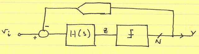
Note that H(s) is a continuous-time filter (s-domain) and there is a DAC in the feedback path to convert from digital back to analog. The comparator shown is a clocked comparator, producing a digital word Y (N-bit).
This article will focus on the choice of architectures for H(s). I will assume the following 3rd-order topology for H(s):
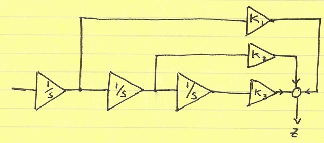
A series of integrators are cascaded and then summed (with weightings k1, k2, and k3) to produce the input z to the comparator. This filter implements
(K1s2 + K2s + K3)/s3
Often times, a noise-transfer zero is desired (to widen the noise-shaped bandwidth); this can be accommodated with the following:
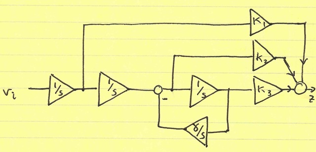
The feedback term γ/s creates a (resonant) pole in the noise-shaping filter which maps to an imaginary zero in the noise transfer function (NTF).
Typically, the active-RC configuration is used for continuous-time filters that are to be tightly controlled and where high linearity is necessary. The first integrator (for example) is composed of a stage shown below:
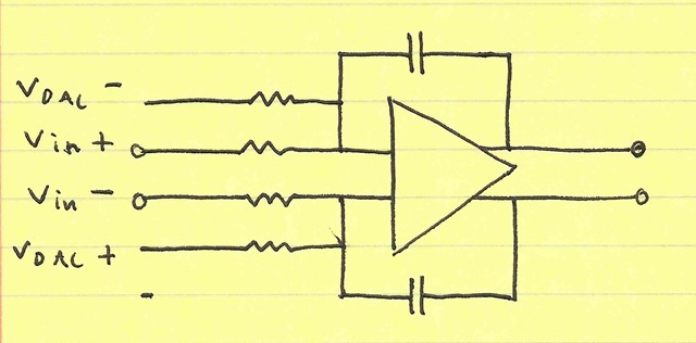
The analog input voltage is converted to a current. Likewise, the DAC feedback voltage is converted to a current. These currents are subtracted into the summing junction and integrated on the capacitor C.
Unfortunately, the main disadvantage of this topology is that the op-amp must now source and sink the DAC current pulse. The response of the op-amp creates an inter-symbol interference problem. The integrated current follows the pulse response of the op-amp. However, when three positive pulses are generated from the DAC, their integrated value does not equal the integrated value of a +1, –1, and +1 sequence of pulses:
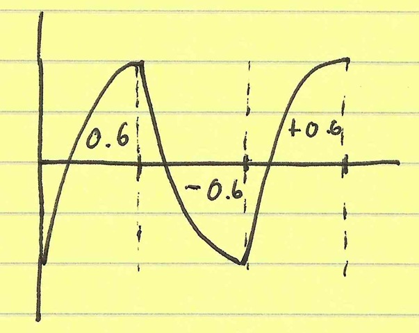 A +1, -1, +1 sequence results in an integrated value of +0.6-0.6+0.6 = 0.6 …
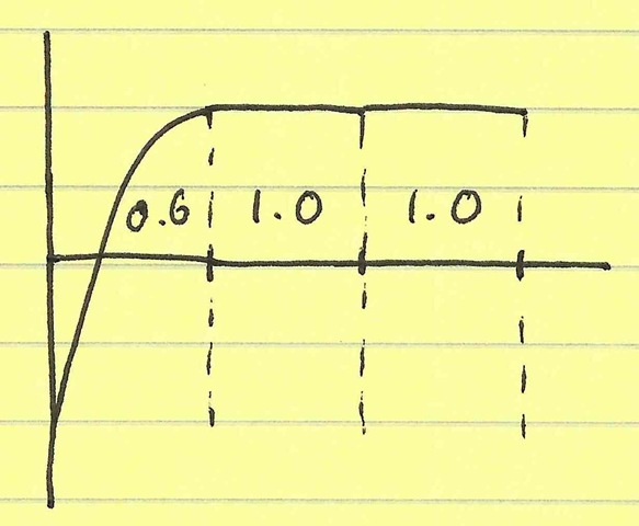 … whereas a +1, +1, +1 sequence results in an integrated value of +0.6+1.0+1.0 = 2.6
In short, the op-amp has an easier time with the DAC maintains a constant output than when it transitions. As a result, the integrated value is signal-dependent, which means it is nonlinear. This effect is worse when the op-amp slews, but occurs even when the op-amp operates in a linear manner.
A popular alternative to the active-RC is the Gm-C architecture:
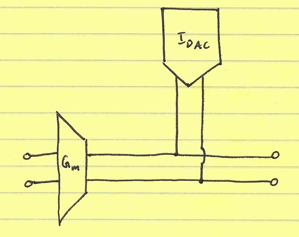
In this case, a (current-mode) DAC’s output is directly summed with the signal current onto an integrated capacitor (which I thoughtfully forgot to draw in the illustration). This architecture isolates the DAC signal from the analog input signal. Consequently, the transconductor requirements are greatly relaxed; it only needs to tolerate the DAC switching on its output, but does not need to actually process the switching signal from input to output.
The main disadvantage of the Gm-C stage is that it cannot drive a low-impedance. Since any resistive loading will steal charge from the load capacitor, only capacitive stages may be driven by the Gm-C stage. Consequently, once one has chosen a Gm-C first stage, all proceeding stages must then be Gm-C—unless one places a voltage buffer in-between the Gm-C and an active-RC.
In the case of the Gm-C, the weighed sum of the integrator outputs must be handled by a separate stage. Essentially, each of the k1, k2, k3 gains would be a separate transconductor that can get wire-summed (summing current) to produce the output z. However, with the active-RC, separate summing stages are not required. By adding a resistor feedback to the active-RC stages, we can allow each stage to pass through a linear term, thus creating a weighted sum of the integrator outputs:
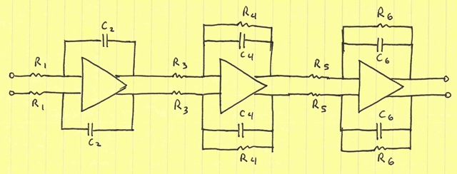
For your clarity and my sanity, I have excluded the resonant γ term. The overall transfer function is
(1/(sC2R1))×(R3/R2 + 1/(sC3R2))×(R5/R4 + 1/(sC5R4))
Which is of the original form
(K1s2 + K2s + K3)/s3
Ideally, one would like the best of both worlds: the ability for the DAC current to bypass the op-amp as in the Gm-C, the voltage-mode output of the active-RC, and the direct weighted sum of the active-RC. It turns out that one can do so by developing a floating DAC that directly sums on the capacitor C1 in the active-RC. To do so, one actually builds two complementary DAC’s that in unison drive each side of the capacitors C1:
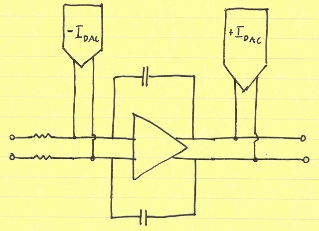
Of course, these DAC’s will not exactly match each other. However, the beauty of this configuration is that when the DAC’s do mismatch, the op-amp can source/sink the current. Nonetheless, if the DAC’s match to 40 dB, we have reduced the high-frequency current demands on the op-amp by 40 dB and increased the linearity by 40 dB.
I had initially thought that this DAC summation method was a novel idea. I don’t have a reference for it, but I am informed that it falls into the class of ideas that are so old they are new.
In the future, I will post another trick one can do to the noise-shaping filter (in combination with what I’ve shown here) that linearizes the continuous-time sigma-delta. Consider subscribing via RSS or email.
[…] a previous post, I discussed the trade-offs in linearity of several continuous-time sigma-delta schemes. In this […]
have a look on Schreier’s publication: a sinc filter has to be added to loop filtering
don’t forget to add capa comm dac because it’s reducing jitterclock constraint..
@Friedel Gerfers:
Thanks for the comment, Friedel. I agree with your comment. A CT SDM is still effectively a discrete-time system (or can be modeled that way). Perhaps I will post about that in the future.
Also, your point is well taken that one can view the CT SDM modulator as an anti-alias filter ahead of the quantizer (albeit with the loop closed around both). Thanks!
Poojan,
please note that a CT SDM is still a discret system due to the sampled quantizer.
Furthermore, since the quantizer is placed behind the CT filter, a CT SD ADC has an inherent anti-aliasing filter.
[…] This post has been updated. Please visit the new location. […]