Introduction
From my personal blog:
I’ve been lucky enough to find myself in a team that’s intent on finding the best circuit design for a given application. This doesn’t happen often to many people, but I feel that I’ve had more than my share of this opportunity.
The conclusion is usually that we come up with some topology (let’s call it circuit X) that optimizes all the performance criteria. I walk away wanting to generalize the experience with the lesson that circuit X is the best circuit ever, and I want to use it everywhere.
Inevitably, I find that some other topology Y is better suited for some other application. There were some specific constraints or conditions on circuit X that don’t apply to circuit Y, and as a result, circuit Y is more optimal for application Y.
It is for this reason that I won’t say that differential circuits are always better than their single ended counter-part. I will say that in my experience, I’ve come across the case where the differential circuit–or, really, the differential approach–is more effective than its single-ended counterpart. However, that’s not why I’ve decided to write this post.
Unfortunately, I’ve come across several engineers that make the generalization error in the opposite direction: they state that single-ended circuits save current. I will present a counter-example that is sufficient to disprove this generalization. Keep in mind that it doesn’t prove the opposite generalization (that differential circuits are always better).
Voltage-Mode Output
The two cases below assume that the dynamic range is limited by output voltage: that is, the circuit will clip its output and that determines the high-end of the dynamic range.
Single-Ended Dynamic Range
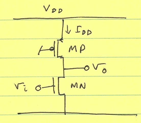
Consider the single-ended CMOS amplifier shown below:

The output noise voltage is given by:
$$ v_{n,o}^2 = \frac{8kTg_m * |Z_L|^2}{3} $$
$$ v_{n,o}^2 = \frac{16 \times kT * I_{DD} * |Z_L|^2}{3*V_{DSAT,N}} $$
The maximum output voltage swing (zero-to-peak) is given by:
$$ V_{o,max} = \frac{V_{DD} – V_{DSAT,P} – V_{DSAT,N}}{2} $$
The dynamic range is:
$$ DR = \frac{|V_{o,max}|^2}{v_{n,o}^2} = \frac{(V_{DD} – V_{DSAT,P} – V_{DSAT,N})^2 \times 3V_{DSAT,N}}{4 \times 16kT \times I_{DD} \times |Z_L|^2} $$
Differential Dynamic Range
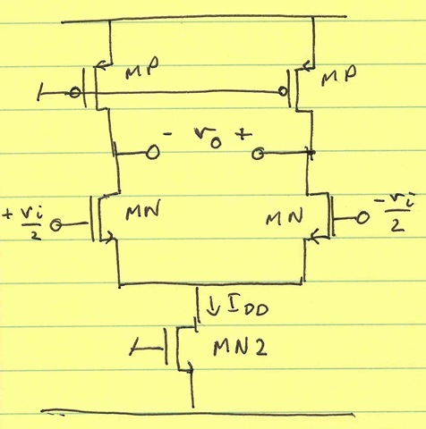
Consider the differential CMOS amplifier:

The output noise voltage is given by (ID is the current in each side of the differential pair; it is half of IDD, the total current):
$$ v_{n,o}^2 = \frac{8kTg_m \times|Z_L|^2}{3} = \frac{16 \times kT \times I_{DD} \times |Z_L|^2}{3*V_{DSAT,N}} $$
The maximum output voltage swing (zero-to-peak) is given by:
$$ V_{o,max} = V_{DD} – V_{DSAT,P} – V_{DSAT,N} – V_{DSAT,N2} $$
The dynamic range is:
$$ DR = \frac{|V_{o,max}|^2}{v_{n,o}^2} = \frac{4(V_{DD} – V_{DSAT,P} – V_{DSAT,N} – V_{DSAT,N2})^2 \times 3V_{DSAT,N}}{4 \times 16kT \times I_{DD} \times |Z_L|^2} $$
Comparison
We see that the dynamic range is equivalent in both cases. The difference is the terms 4(VDD – VDSAT,P – VDSAT,N – VDSAT,N2) in the differential case versus (VDD – VDSAT,P – VDSAT,N) in the single-ended case. In many cases, the differential dynamic range is larger. In fact, as long as
$$ V_{DSAT,N2} < \frac{3}{4}(V_{DD} – V_{DSAT,P} – V_{DSAT,N}) $$.
However, in the case where you can’t meet this requirement, you can get rid of MN2 (albeit at the cost of common-mode rejection).
Conclusion
We’ve seen a case where the differential circuit shows more dynamic range than the single-ended counterpart. My guess is that most people who say that differential means more current don’t realize that you don’t have to have the same current in each branch of the differential circuit (you can split the current in half).
One limitation of the above analysis is that I assume that the input voltage is available in a differential form, and that the output is consumable in its differential form. Obviously, if this isn’t the case, the above analysis may or may not work. The case becomes more specific and the generalization fails.
That said, I’ve seen plenty of line-ups where a transformer/balun is placed off-chip to convert the chip’s inputs/outputs to differential. Requiring differential I/O at the chip level doesn’t mean requiring differential I/O at the board level.
Current-Mode Output
I’ve detailed the use of current-mode circuits before. It’s possible to treat this as a special case of the voltage-mode output analysis, with ZL being small. The only problem with that extrapolation is that if ZL is small, the maximum swing probably won’t be dictated by voltage: the circuit will slew way before it clips. As a result, instead of Vo,max being given by the previous equation, we have:
Single-ended:
$$V_{o,max} = \frac{\alpha \times I_{DD} \times |Z_L|}{2}$$
Differential:
$$V_{o,max} = \alpha \times I_{DD} \times |Z_L|$$
where α is a factor that indicates what fraction of quiescent current can be used as signal current.
The advantage is even more apparent: you’re getting 4× the dynamic range.
Additional Benefits
In addition to the improved dynamic range (power-drain efficiency), differential circuits offer:
- Reduced susceptibility to supply noise: a good chunk of supply noise appears as common-mode, so a fully-differential circuit will reject (ignore) it
- Improved IM2: IM2 generally appears as common-mode and to a large amount gets rejected
- Reduce supply bounce (more beneficial for switch-mode circuits): since there’s a complementary action at the nodes in the differential circuit, much less noise is induced on the supply during dynamic operation
Disadvantages
I can only point out a few disadvantages to the approaches presented here–and they really have nothing to do with single-ended (versus differential) circuits:
- Common-mode feedback: you’re generally going to need a common-mode feedback (and common-mode sensing). However, even the single-ended topology (shown above) requires some bias adjustment to set its output bias voltage. This is more of a property of CMOS design (high-impedance loads) than a trade-off of single-ended/differential circuits.
- Lower swing: once again, this is a property of the differential pair. But, a lot of the differential benefit (common-mode rejection ratio) comes from using the differential pair.
True disadvantages:
If you’re using minimum-size devices, you end up spending twice the current with the differential circuit than with the single-ended version. However, when (in analog design), have you used minimum-sized devices?
The benefits of differential circuits occur when you get to analyze the noise and signal swing differentially. However, if the circuit you’re driving doesn’t respond to a differential input, the benefits aren’t as great.
Conclusion
It seems to me that most of the people that globally avoid differential circuits subscribe to the thought that since there are two current branches, there must be double the current. However, like I said above, this is only true if your branches are using minimum-sized devices. Otherwise, you can always split the device in half and distribute the same current across a differential pair.
[…] « The benefits of differential circuits Special thanks to Justin Patrin » […]
Good discussion. In my experience, differential circuits nearly always have more significant benefits than single ended circuits. The big one in ICs using single ended circuits is the risk of unknown spurious signals coupling into a critical circuit through the substrate, package etc, and potentially destroying performance. This makes common mode rejection is a huge plus. In my mind, the primary drawback to differential circuits is layout complexity. If the required SNR for a circuit is low, and I want to minimize complexity, that is when single ended circuits have a niche.
I completely agree with Mark’s statement. CMRR is the single most important criteria that makes the differential circuits stand out. If a circuit can correctly operate at lower SNR, single ended circuits would be fine. Differential circuits also impose upon layout to be symmetrical especially the difference sensing amplifiers and noise coupling or noise shielding structures.