In this post, I will show an evolution of a trans-conducting LNA (rather than a voltage-gain LNA). This is a prime example of current-mode circuit design, which has benefits in terms of linearity—especially for low-voltage scaling in RFCMOS design.
Conventional common-gate LNA
Consider the conventional common-gate LNA on its own:
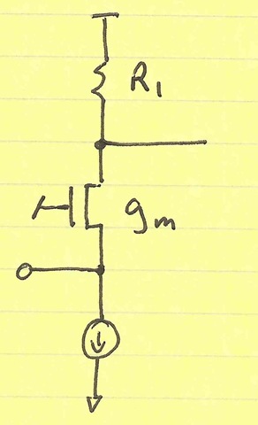
This LNA consists of an input at the source of the MOS transistor (or emitter of a BJT) , a current-source to bias the transistor, and a resistor load. This configuration is typically used in broadband receivers (cable tuners, TV tuners, software-defined radio).
The gain of this stage is Av = gm×R1. This seems like a reasonable stage to produce a gain and therefore overcome noise.
Each of these circuits is presented as a single-ended version. However, there is absolutely no reason not to implement them as differential circuits. I merely draw them single-ended here to get the point across without obfuscating the primary ideas. If there is interest in seeing what the differential versions look like, please post a request in the comments section.
CMOS LNM employing voltage-mode LNA
However, consider what happens when we couple this LNA into a CMOS switch-mode mixer:
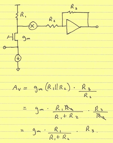 The ⊗ symbol represents a set of commutating MOS mixers, typically capacitively coupled, to separate the dc bias voltages at the output of the LNA and the input of the post-mixer amplifier (PMA). You can essentially ignore then in this analysis, and just assume that they ideally convert from RF to baseband (direct conversion).
Consider the loss term R1/(R1 + R2). It doesn’t have to be there.
Trans-conducting LNA
If we replace R1 with a current-source load and merely omit R2, we’d have something like this:
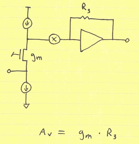 You’ll note that the previous loss term is now gone. We have greatly enhanced the gain at essentially no cost. Furthermore, the resulting architecture is even more linear: there is little swing at the output of the LNA; the summing junction of the PMA linearizes the LNA by presenting a low impedance to the LNA.
Due to the high output impedance of the LNA, a common-mode feedback circuit is necessary. I have detailed two ways of doing that.
References
Matt Miller and I came up with these ideas at Motorola in 2004. We were not the only ones. Other people within Motorola came up with the same idea. In addition, I had seen it published somewhere around 2004—I thought by Michiel Steyaert or Thomas Lee. Despite my recollection, the closest references I have seen available are: “A 72mW CMOS 802.11a direct conversion receiver with 3.5dB NF and 200kHz 1/f noise corner” (albeit using an inductor load instead of PMOS loads) and “A 1 V 1.1 GHz CMOS integrated receiver front-end” (with a folded Gilbert cell mixer).
[…] detailed the use of current-mode circuits before. It’s possible to treat this as a special case of the voltage-mode output analysis, […]
hi poojan,
i love your analog desgn insight posts.
‘current mode design’ is a bit of a black art for me. and there is only ONE book in entire Amazon on it !
Can you pl write an article on rough rules of thumb to use for (1) when to use current mode and (2) how 2 go about designing in current mode.
can you pl also write a post on why the OTA [operational trans-conductance amplifier] failed to ‘take over the world’ ? what caused its demise ? and is it still used in some neiche ? what is that neiche ?
I know about the 4-20 ma current loop of Induatrial, and the teleco current loop for POTS onhook-offhook detection.
ashvini, new delhi , india.
@Robert Tso:
You’re right about the impedance going high outside of the gain-bandwidth of the op-amp. Typically, you’ll want to put a capacitor on the inputs of the PMA to maintain a low impedance when the PMA’s op-amp (OTA) runs out of steam (and to suck out any LO injection). The addition of such a capacitor is not trivial as it can really screw up stability.
I also recall that there’s a filter configuration (was it Tow-Thomas?) that includes such a capacitor.
I will admit ignorance on many of the details of the BBF, because there was either someone else to do that job (which, I will admit, is the crux of this configuration), or I was always pulled off to other tasks.
If the post mixer amplifier is a low bandwidth amplifier, then it will not do a very good job in presenting a low impedance at the mixer output or at the gm stage output, – so the benefits of improving gm stage linearity would not be realized
The likely advantage of the 2nd schematic configuration is that it allows a filter to be placed between the mixer and baseband amp.