In this post, I will detail how I designed a regulator quickly. The idea here wasn’t to get the best performing regulator, but just one that did the job.
I do care about performance, area, and power, just not as much in this case. The most important thing was to meet the schedule. If I didn’t have a regulator, I would have no ADC to measure. So, any regulator was better than no regulator.
After I was done, I realized that the result was a really good basic regulator—one that someone could design quickly, and then build upon to realize something more optimal.
The regulator was meant to power the comparator in a sigma-delta ADC. This comparator (the load circuit) is comprised of both analog (constant-current) and switching circuits. The analog section impinges very little on its supply. We therefore focus on the switching portions of the load circuit.
Switching Circuit Load
Before we consider the design of the regulator, let’s consider how a switching circuit draws power from its supply.
Take the switching diagram of an inverter with a capacitor load $C_L$, shown below:
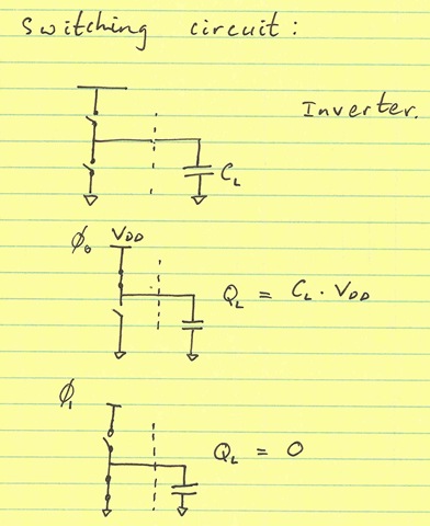
This circuit dissipates current from the supply in two steps. In the first phase ($\phi_0$), the upper switch connects the load to supply. A charge of QL=CL*VDD has been sourced from supply. During the second phase ($\phi_1$), this charge is taken off the load capacitor and dissipated to ground.
Regulator with Switching Load
Let’s for now model the regulator as a fixed resistor between supply (VS) and its output (VR). Note that VR is also the supply to the switching circuit.
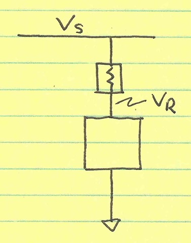
This model is valid for cases when the feedback loop of the regulator isn’t fast enough to correct the output voltage. This short/quick transient is exactly what we’ll consider here.
During the phase ($\phi_0$) when the inverter pulls charge from supply, there’s essentially an RC formed between the supply VS, the resistance of the regulator, RR, and the load capacitor CL. The regulated voltage takes a dip down and settles back:
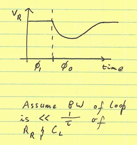
This is obviously a bad situation: the regulated output takes a large droop. In the case of my comparator, this would definitely effect the linearity, since the droop in supply would be signal-dependent.
Here’s the dirty little secret: for RF circuits and high-speed circuits, the regulator is too slow to do anything about these switching transients. The regulator feedback can do nothing to correct this droop.
The Regulator Bypass Capacitor
To alleviate this droop problem, we put a capacitor on the regulator’s output:
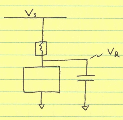
Instead of sourcing charge through the regulator resistance, the charge can come off the bypass capacitor CR.
Now, we have a switched-capacitor circuit. The load capacitor of the regulator is now connected to CR. Take, for example, the case where CR is 10x CL, the regulated output is 1.0 V, and the inverter starts out with a low (0 V) output:
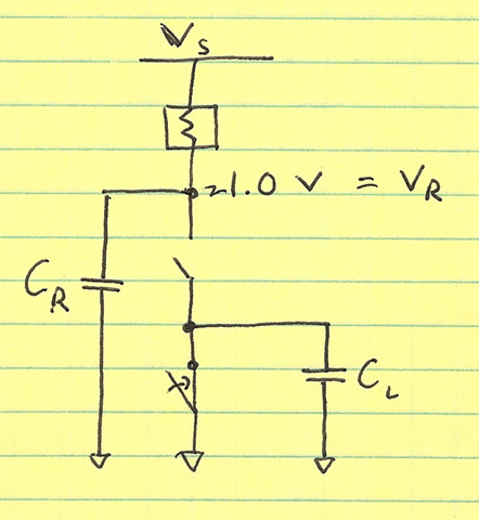
When the inverter output now goes high, we have charge sharing between the load capacitor CL and the bypass capacitor CR:
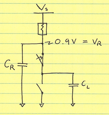
Since the load capacitance is 10% of the bypass capacitance, 10% of the charge is transferred from the bypass capacitor to the load capacitor, and we get a 10% drop in the regulated output.
More generally, if we design CR to be $F \times C_L$, we will generally see a $\frac{1}{F+1}$ droop in our regulated supply VR.
An Effective CL
Obviously, our circuit does not consist of a single inverter. So, how do we estimate CL? The method I use is to vary the switching frequency. If there is a clock that determines the frequency of $\phi_0$ and $\phi_1$, we can use that to determine the effective CL by varying the clock frequency. Recall that during every clock period, we above circuit dissipates a charge QL = CL*VR from VR.
So, we have a relationship of current with switching frequency:
$$I_R = I_{R0} + C_L \times V_R \times F_S$$
$I_{R0}$ represents the current drawn by analog (constant-current biased & simple resistor) elements within the load circuit. We can back-solve for an effect $C_L$ by looking at the change in $I_R$ from a (say 10%) change in $F_S$:
$$\Delta I_R = C_L \times V_R \times \Delta F_S$$
$$ C_L = \frac{\Delta I_R}{V_R * \Delta F_S} $$
So, let’s for example consider the following table extracted from simulations:
| FS | IR |
| 100 MHz | 5 mA |
| 110 MHz | 5.1 mA |
$$ C_L = \frac{0.1 \text{mA}}{1.0 \text{V} * 10 \text{MHz}} = 10 \text{pF} $$
I wanted to make sure that my regulator supply (VR) was rock solid. So, I chose CR to be 100 X 10 pF = 1 nF. (Like I said, I didn’t care that much about area in this case.)
[…] supply droop can be alleviated by sufficient bypassing. The problem and solution follow identically my previous post on supply regulation except that in that case of a feedback regulator, the low on-resistance is more […]