In Part 1, I discussed how the regulated supply reacts to a switching transient, and how the regulator bypass capacitance CR suppresses the transient.
In this post, I will discuss how this same bypass capacitance affects the loop gain characteristics of the regulator. I will then present a procedure to design this regulator quickly, and stabilize it after the fact.
Regulator Schematic
Here’s the full schematic of our regulator:
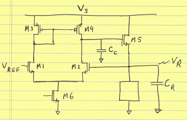
M5 is the regulating device. The diff pair is an OTA (operating transconductance amplifier, but also referred to as an op-amp despite its high output impedance) that implements the feedback (with a lot of gain). If more gain is desired, devices M1/M2, M3/M4 can be cascoded. M6 can be cascoded for better CMRR (common-mode rejection ratio).
There are two poles to consider in this feedback loop. The dominant pole (by design) is at the drains of M4/M2. It is:
$$\frac{g_{ds2} + g_{ds4}}{C_C}$$
The non-dominant pole is:
$$\frac{g_{m5}}{C_R}$$
(Note that if the circuit being regulated has any supply capacitance, it should be included in CR).
The dc loop gain is (approximately–excluding the output resistance of M5):
$$\frac{g_{m2}}{g_{ds4}+g_{ds2}}$$
To maintain phase margin, we want the dominant pole to be well below the non-dominant pole.
The regulator output capacitance CR has already been defined in Part 1. Since this is a quick-and-dirty design, we will simply size CC after the fact so that we get adequate phase margin.
Sizing Devices
We presume that there is a current specification on the OTA, so the bias for M6 is already defined. Obviously, more current is always better (more loop bandwidth).
Devices can be sized as follows:
M5
We size M5 to provide some minimum non-dominant pole frequency. This non-dominant pole frequency (and some phase margin specification) dictates our dominant pole frequency and therefore dictates the bandwidth of the loop. We won’t worry about loop bandwidth in this design. We will just live with what we get.
If there is variation in IR, the current going into the load circuit, then this pole frequency needs to be specified with the minimum current. This low-IR extreme is the limiting case on stability. When the current in M5 increases past this minimum, $g_{m5}$ increases and the non-dominant pole simply increases in frequency, making the system more stable.
M3/M4
The gate of device M5 is at VR + VGS5 = VR + VT5 + VDSAT5. So, we size M3/M4 to have:
$$|V_{DSAT3/4}| < V_S – (V_R + |V_{GS5}|)$$
Making M3/M4 large will cause |VDSAT3/4| to be low but will also lower the frequency of the dominant pole and will also reduce the dc loop gain.
This consideration on the drains of M3/M4 indicates a limitation: if the quantity VR + |VGS5| is too close (or higher than) VS, we cannot design a regulator using this topology. For example, if VS is 2.5 V and VR is 1.8 V, and a threshold is 700 mV, we don’t have enough headroom because VR + VT5 will be 2.5 V. The drain voltage of M4 (VR + VT5 + VDSAT5) will be higher than VS (2.5 V).
In one case, this limitation caused me to make M5 a thin-oxide (rather than the thick-oxide I/O device commonly used for analog design). The thin-oxide devices have a much smaller threshold voltage, greatly reducing the drain voltage on M4. An alternative option is to use a 0-VT (sometimes called native) device for M5. That option wasn’t available to me.
M1/M2
M1/M2 can be sized for loop gain. Increasing M1/M2 increases the loop bandwidth up to a point. Past that point, the gate capacitance of M2 dominates CR.
Recall that gm2 is proportional to $\sqrt{W_2}$. However, Cgs2 is proportional to W2. So, there is a losing battle as Cgs2 increases faster than gm2.
M6
M6 is simply designed (like in any other diff-pair) to be a good tail current source. The drain voltage on M6 is:
$$V_R – V_{T1/2} + V_{DSAT1/2}$$
VDSAT6 should be sufficiently lower than this drain voltage.
Stabilization
Finally, after doing all of the above, we can measure the loop gain. If there is no phase margin, we simply size CC higher to get some phase margin.
For example, if the loop gain looks like this:
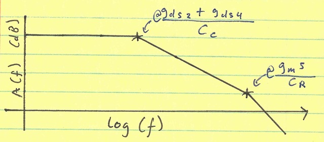
we can increase CC to shift the dominant pole in and make it look like this:
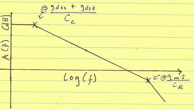
Note that doing so does not affect the dc gain. However, it does affect the 3-dB loop bandwidth. This 3-dB bandwidth will likely end up being in the kHz or MHz range. Nonetheless, between this 3-dB bandwidth and the unity-gain frequency (likely 100’s of MHz to single GHz) there still is some (and likely considerable) loop gain.
Further optimization
A more optimum design might modify devices to improve loop bandwidth. This could be done by re-sizing M5 to increase the non-dominant pole which would allow the dominant pole (and 3-dB bandwidth) to be extended. Alternatively, device M5 and the capacitors could be optimized for supply isolation.
The design procedure presented in this post is an excellent starting point for such optimizations.
Summary
- Deciding on a bypass capacitance CR
- Sizing devices as necessary for the minimum IR case
- Designing CC for stability
I welcome your comments and questions.