I received a request to go through the design of a flip-flop. Every flip-flop I have designed has been a master-slave D flip-flop, built out of two D latches. I’ll start with a basic CMOS latch and go into more optimized latch topologies.
Update 2008-12-19
This post probably didn’t make sense to many of you. I was representing C-bar (negation of C) by and underline. Unfortunately, WordPress (or maybe my theme) wasn’t rendering this underline, so $\overline{C}$ didn’t look any different from $C$. I’ve (obviously) rectified this ambiguity through the magic of Latex. If there are any errors now, they are solely my fault. (Let me know.)
Consider the cross-coupled inverters shown below:
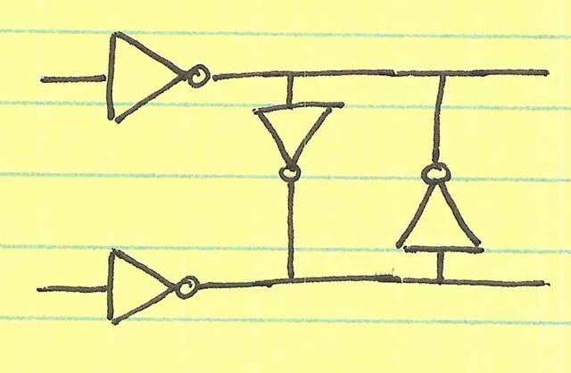
The two inverters chasing their tail to the right of the input inverters represent a memory unit (i.e. a latch). When one output is high the other one is forced low. This low output then reinforces the first output being high. These two inverters form a positive feedback system.
I will represent almost all circuits as fully differential. That is generally how I’ve encountered these structures, and it also more general. If one wants a single-ended version, simply lop off one of the input structures (but keep the cross-coupled inverters).
This system has two stable states: the top output high (at supply) and the bottom output low (at ground) or vice versa. One additional trait of these cross-coupled inverters is that it takes a bit of effort to flip them from one state to the other. One must essentially cause the top output to go from high to low by overcoming the inverter driving the top output. In other words, the input inverters (on the left) must be sized larger than the cross-coupled inverters.
Our desire, however, is not to have the state change at random. We want the latch state to change only upon the transition of an external clock. This can easily be accomplished by passing the input inverter’s output through a transmission gate controlled by the clocks $C$ and $overline{C}$.
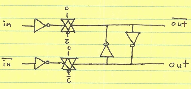
Now, we have a true latch. I won’t repeat Wikipedia in analyzing a flip-flop as two successive latches triggered on opposite phases of the clock signal.
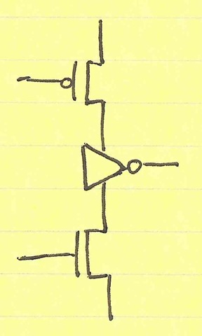
Now, let’s look closer at the inverter and T-gate combination in more detail:
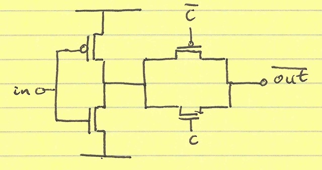
The PMOS controlled by $\overline{C}$ does very little when the output of the inverter is low. It is basically there for pull up. Similarly, when the inverter output is high, the NMOS controlled by $C$ does very little; it is basically there to pull $\overline{out}$ low. As a result, we can lose the connections between the PMOS and NMOS in the T-gate and incorporate the T-gate into the inverter:
This structure has the advantage of allowing an contact-less diffusion between the series PMOS devices and another contact-less diffusion between the series NMOS devices, as I illustrated in the MOS diffusion parasitics article.
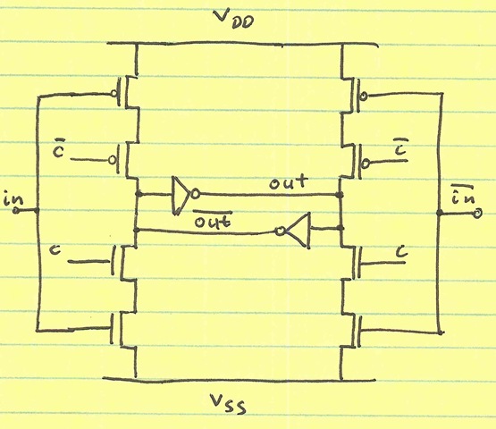
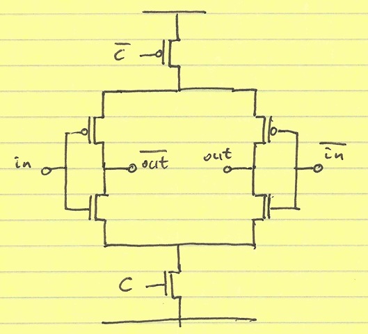
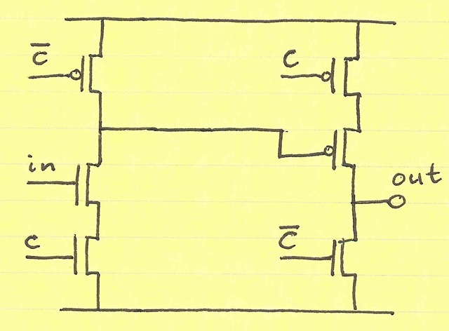
Another manipulation we can perform on this structure is to reverse the roles of input gates and clock gates (switching the connections of $in$/$\overline{in}$ and $C$/$\overline{C}$):
Note that while both PMOS clock devices (driven by $ \overline{C} $) are turned on, only one is actively pulling up an output. For example, the PMOS devices on the left pulls $ \overline{out} $ up when $in$ is low. However, the upper right PMOS device (driven by $\overline{C}$) does nothing because the PMOS in series with it is off ($\overline{in}$ is high).
I will draw this structure as a gated inverter in the future:
Up to this point, the input structure has always had to fight the memory effect of the cross-coupled inverters. Essentially, the input structure must inject enough current into the cross-coupled inverters to force them to switch states. This contention can result in considerable power draw. This power draw can be alleviated by gating the cross-coupled inverters (enabled on the opposite phase than that of the input structures):
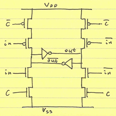
Finally, the PMOS clock devices can be combined into one device; and the NMOS clock devices (driven by $C$) can be combined into one device. I have omitted the cross-coupled inverter devices for brevity:
Doing so has the benefit the PMOS clock device can be twice as large while maintaining the same capacitive load on $\overline{C}$. Similarly, the NMOS clock signal $C$ can see the sum of the device widths from the previous configuration yet whichever NMOS is on ($in$ or $\overline{in}$) is now in series with a device twice as wide.
Finally, one can omit some level of gating by pre-charging the latch. That is, instead of waiting for the input to determine whether we pull the output high or not, we pull the output high during the first half of every cycle. During the second half, we pull down only if the input should really be low. The following flip-flop structure achieves this pre-charging. Once again, I have omitted the cross-coupled structures:
The first stage’s PMOS pulls up whenever $\overline{C}$ is low on every cycle. Then, on the next half-cycle (when $C$ is high) the NMOS pulls down only when $in$ is high. Since the first stage only has one PMOS device (rather than two in series), the pull-up action is faster. Since we want to clock the second latch stage on the opposite phase (to form a full flip-flop), we need to invert the pre-charge and pre-charge low (rather than high).
The main problem with the pre-charge architecture as shown is that the first stage (for example) pulls up on every cycle even when the input $$in$$ is always high (and the output should be low). This represent a great deal of charging and discharging on the output of the first stage and thus dissipates power. However, this represents a fundamental trade-off: that one can gain increased speed at the expense of power.
[…] simplest of these is to insert more latching stages within the loop. These latches as I’ve discussed before utilize positive feedback to gain up the signal and force a hard binary decision. The penalty is […]
very good tutorial on cmos based latch design
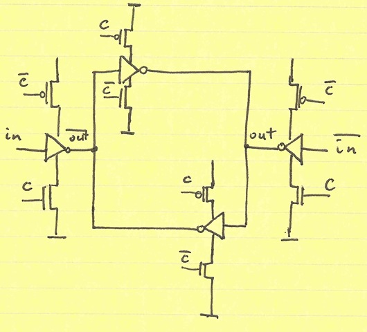
This is an unusual D-flop design which I wasn’t familiar with. I wrote up a Spice deck and compared the perf with a regular D-flop design at http://www.vlsitechnology.org/html/cells/vsclib013/dfnt1.html. The new one is at http://www.vlsitechnology.org/html/cells/vsclib013/dfnt2.html.
In the case of single date and clock inputs and a single output, I can’t see the advantage of this design. It’s very big (34 transistors cf 24 for the regular flop) and uses more power for a slower speed. I also found bigger setup and hold times.
The parasitic caps are estimates since I haven’t drawn a layout. I think it will be complex, with the nodes n1p,n1n thru n5p.n5n being tricky because continuous diffusion isn’t possible.
Is the schematic I have drawn correct?
@Graham Petley:
Hi, Graham. Your schematics look correct to me. As you stated, the real implementation benefit of this configuration is in a fully-differential configuration, where I get to divide the power in half (or to put it another way, where I’d have 2 single-ended latches anyway).
The other benefit of this design is that it has an evolution from the basic latch configuration, which serves as a good introduction to the workings of the latch.
I will admit that as an analog/RF engineer, I haven’t really strayed outside of these (or similar) latch designs, as a fully-differential topology is strongly preferred, due to lower clock-induced supply bounce. These designs favor 50% duty ratio outputs over power efficiency. Of course, the majority of people don’t care about duty ratio and matched rise/fall times.
I don’t claim that it’s an optimal general purpose latch–but it does its job at rather high frequencies.
Very nice tutorial.
@mm: Thanks for the heads-up. I foud out that WordPress (or its Carrington theme) wasn’t rendering underlines (which I was using as a proxy for overbars). Luckily, with a web version of Latex, I a now able to represent both C & C-bar.
@mm: You are correct; I have C & C-bar reversed in the description. I’ll fix it when I get a chance.
It looks to me as if clock phases driving PMOS devices in the pre-charge type circuit were reversed. To make the circuit work as described, first stage should be driven with “C” and the second one with “/C”.