I was asked a question on how to reduce leakage for digital circuits. I started by detailing process options that effect leakage, each effective both leakage and circuit performance. In this article, I will detail two methods to reduce leakage while maintaining circuit performance. I assume that the circuit at hand requires the highest performance in some active mode but must greatly reduce its leakage in a standby mode.
Supply Switch
The simplest method to reduce leakage in standby is to provide a switch to supply that opens during standby. Since the sea of digital devices are then disconnected from supply, their gates cannot be at supply and therefore their gate leakage goes away. In this case, I have represented the sea of gates as an inverter, with its supply and ground connections explicitly shown:
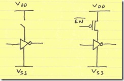
The bigger concern is active operation. The PMOS switch has some finite on-resistance. Current spikes during the transition of the digital circuits will cause voltage spikes on the supply of the digital circuit as Ohmic loss builds through the PMOS switch. In effect, the PMOS switch reduces the pull-up capability of every gate in the digital circuitry:
This transient supply droop can be alleviated by sufficient bypassing. The problem and solution follow identically my previous post on supply regulation except that in that case of a feedback regulator, the low on-resistance is more frequency-dependent than with the PMOS switch. To keep the static supply droop under control, the PMOS switch should be made adequately wide. Doing so can cause the supply switch to have a size on the order of the entire digital circuit area.
Reverse Body Bias
The back-gate or body can also be used to reduce leakage. Essentially, leakage gets reduced when the threshold is increased—decreased (increased in magnitude) for PMOS devices. Biasing the body below the source for NMOS or above the source for PMOS can increase the magnitude of the threshold voltage.
To do so, we allow two connections for the body. I have picked the PMOS case for the body switching because typically, there is one ground available but two supplies (a higher-voltage I/O supply and a lower-voltage core supply):
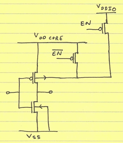
When the enable EN signal is asserted high, EN will be low and therefore turn on the PMOS device that ties the body of the core circuit’s PMOS device to VDDCORE. When EN is deasserted low, EN will be pulled high and turn off this connection. In its place, the secondary PMOS device will pull the core body connection to VDDIO, effectively increasing the magnitude of the Vt of the core PMOS device, and thus reducing leakage in the inverter.
The main difficulty with the above technique is that it requires a separate connection for the PMOS body. Typically, in standard cell logic, the body is directly connected to supply.
There is also a risk that if these body-connecting PMOS devices have too large of an on-resistance, they can cause latch-up. Care should be taken to ensure that the on-resistances of these deices are low. However, the size of the resulting PMOS devices in this case would still be much less than that required of an equivalent PMOS supply switch.
One of the main benefits of the reverse body bias technique is that it allows for circuits which hold state (static memory cells). This is out of my range of experience, but it may also improve the required refresh rates on dynamic memory cells, too—thus slowing down refresh clock rates and therefore greatly reducing power.
Dear Poojan,
I agree that reverse bias helped in the “good old days” of process nodes like 180nm.
But if you simulate the bulk effect in e.g. 45nm, you will see that the 1000x Ids leakage reduction in 180nm will shrink to <10x best case in 45nm.
On top of the Ids leakage, gate leakage gets more pronounced!
Thanks
Friedel
@Bapcha Murty:
I concur. I think the high-side switch is the way to go. However, there are some benefits of the reverse body bias. I just wanted to give as many options out there as possible for my readers and let them decide. Their decision, nonetheless, should be to just use a switch 90% of the time.
Could you explain what you mean by increasing sidewall capacitance?
1. Reverse body bias will require that you do a custom layout to minimize the chances of latching up – plus, you will end up increasing CJSW [side-wall capacitance].
2. Stacking devices – as in the supply switch circuit – will decrease DC power and standby power, but you need LARGE enable transistors to implement a high-speed circuit.
Intuitively, I think that using the reverse body bias to eke out better performance is a bad engineering trade-off to make, while I’d be more comfortable with the switched power supply solution.
Bapcha
[…] unknown wrote an interesting post today onHere’s a quick excerptMost recently, he is working in the areas of analog-to-digital converter design in […] Share and Enjoy: These icons link to social bookmarking sites where readers can share and discover new web pages. … […]
[…] Of course, each of these options have the implicit tradeoff of performance/speed at the expense of leakage. What do you do when you want performance during active operation and low leakage during a standby mode? I will detail two methods in a future article. […]